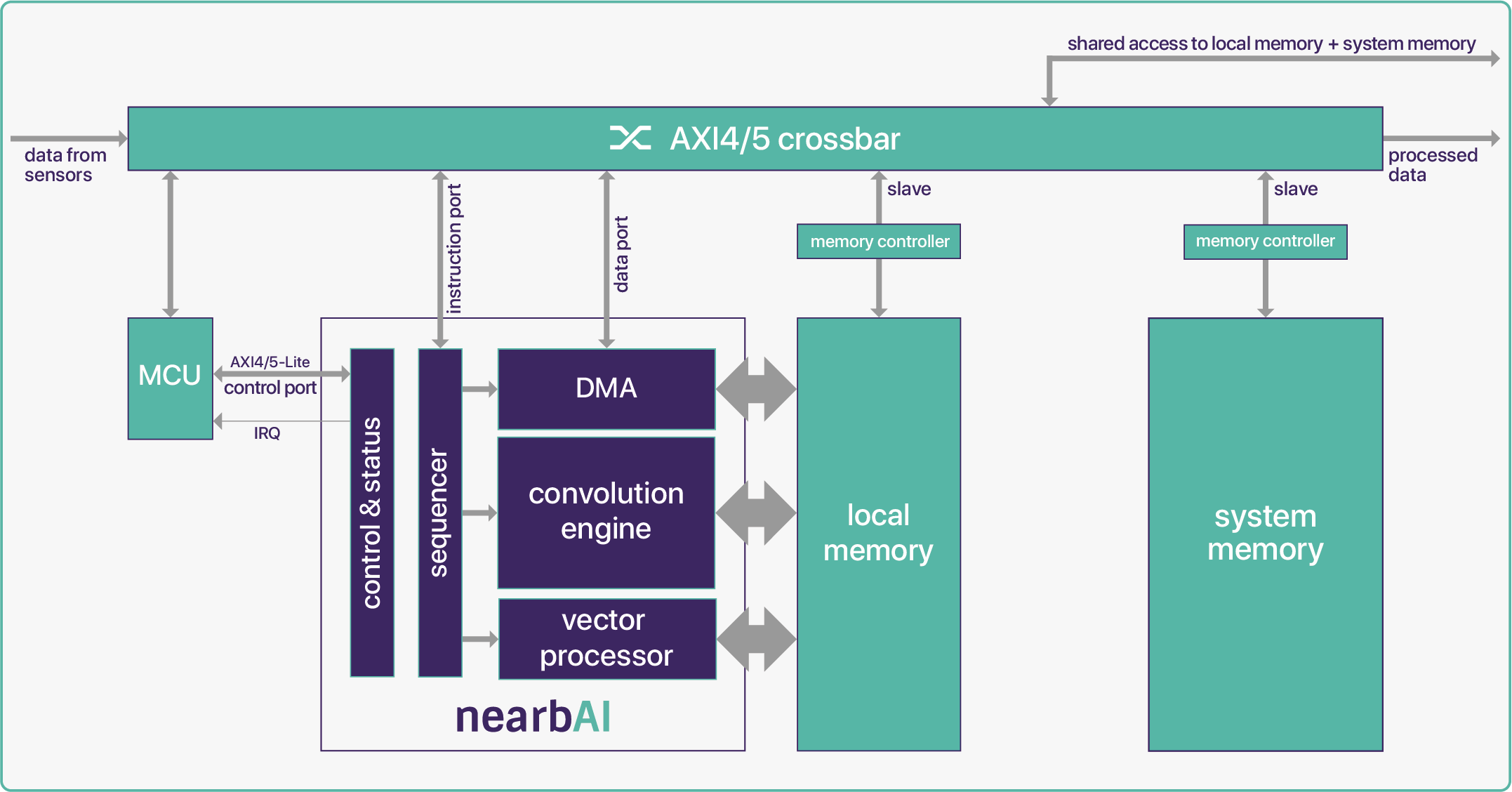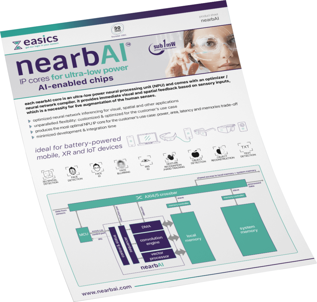

each nearbAI core is an ultra-low power neural processing unit (NPU) and comes with an optimizer / neural network compiler. it provides immediate visual and spatial feedback based on sensory inputs, which is a necessity for live augmentation of the human senses.
optimized neural network inferencing for visual, spatial and other applications
unparalleled flexibility: customized & optimized for the customer’s use case
produces the most optimal NPU IP core for the customer’s use case: power, area, latency and memories trade-off
minimized development & integration time
answers to your needs
ultra-low power
- maximized battery performance
- supports battery-powered always-on applications with wake-up
- does not have to transport full video signals from the sensors as it supports local processing
zero-latency switching
- continuous multiplexing between multiple neural networks, on the same nearbAI core
- one neural network detects regions-of-interest and passes them to the next network, on the same nearbAI core, example: feed detected faces into face recognition network
local processing
- each nearbAI operates standalone:
- ultra-low latency
- privacy conserving: local removal of sensitive data
- high level of data security and reliability
scalable & flexible
- optimized power-performance-area (PPA), based upon customer needs
- silicon technology agnostic: 40nm down to 4nm and beyond
- programmable using the optimizing compiler during the product lifecycle
optimizing nearbAI compiler
- reads in your neural network in ONNX format using TensorFlow, Keras, PyTorch, mxnet
- includes profiler with full layer-per-layer visibility
- single-bit granularity data types
time-to-market acceleration
- very fast FPGA prototyping in path towards ASIC
- smooth integration of the easics IP core
- efficient deployment and field upgrades via OTA
ultra-fast response time
- live feedback within response time of human senses, from sensors to in-glass displays
- real-time pattern recognition with fixed inference latency; face detection in 2 milliseconds
unique small footprint
/low cost
- smallest silicon area
- lowest ASIC cost and lowest PCB cost
- no additional XR accelerator chips needed
easy SoC integration
- application & integration templates available
- supports Linux API & bare metal
- peripheral and sensor interface blocks supported
- support & integration team with +30 years experience / first-time right
secure OTA updates
- field upgrades of neural network models and weights using secure SW over-the-air updates
- lifecycle management
- supports offload engine/processor outside IP core
function examples
3D / spatial
detection
face
detection
face
ID
face
blurring
iris
ID
gesture recognition
/hand tracking
object
detection
object
reconstruction
text
detection
why nearbAI?
highly computationally efficient and flexible NPUs
enable lightweight devices with long battery life ... with ultra-low power, run heavily optimized AI-based functions locally
enable truly immersive experiences ... achieve sensors-to-displays latency within the response time of the human senses
enable smart and flexible capabilities ... fill the gap between “swiss-army knife” XR / AI mobile processor chips and limited-capability edge IoT / AI chips

optimizer platform for ASIC
the L3 optimizer is a powerful ASIC optimizer platform that specializes in optimizing low power, low area, and low latency use cases for our customers. with the L3 optimizer, customers can expect customized solutions that are tailored to their specific needs, resulting in superior performance, reduced power consumption, and minimized area usage.
nearbAI is unique, delivering best-in-class solutions for battery-powered mobile, XR and IoT devices. It builds on more than three decades of DSP and image sensor chip design. Our mission is to provide customers with IPs that perfectly fit their specifications, offer outstanding performance, and are seamless to integrate right through to tape-out.
easics is committed to bringing the most advanced technology and solutions to market. With nearbAI, along with our partners and customers, we are pushing the latest AI innovation to the extreme edge
easics is committed to bringing the most advanced technology and solutions to market. With nearbAI, along with our partners and customers, we are pushing the latest AI innovation to the extreme edge

ramses valvekens
CSO & managing director
easics
easics
let’s do a custom benchmark together
provide us with your use case:
quantized or unquantized NN model(s):
ONNX, TensorFlow (Lite), PyTorch, or Keras
constraints:
average power & energy per inference, silicon area, latency, memories, frame rate, image resolution, foundry + technology node

first-time right
we are also offering:
feel free to get in touch with us
complete the form below and we will contact you within 48h
start the collaboration with us
and we will deliver the best solution
based on your needs
and we will deliver the best solution
based on your needs
easics nv
diestsevest 32 box 2b
3000 leuven, belgium
diestsevest 32 box 2b
3000 leuven, belgium
vat: BE 0444.501.015
services
products
© 2024 easics NV. All Rights Reserved – Privacy Policy


